Technology Innovation
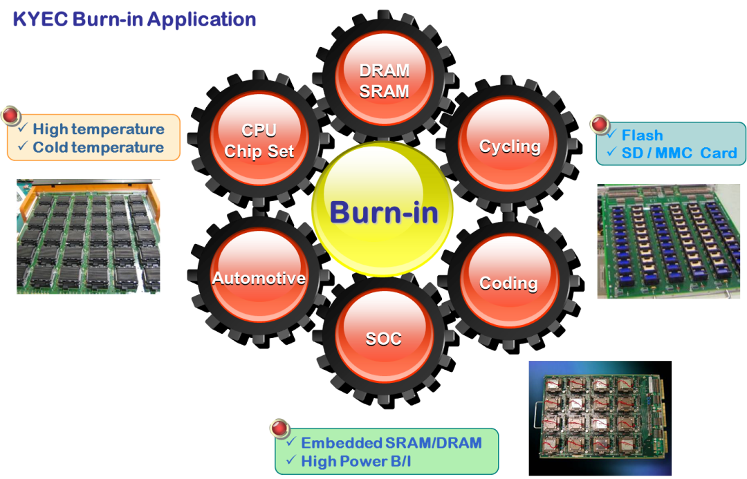
The Burn-In Oven technology developed by KYEC can be used for a variety of applications, from central processing units (CPU), thin film transistor liquid crystal display (TFT LCD) and gaming console products to today's memory products, power ICs, automotive ICs and Light-Emitting Diodes (LEDs), etc.
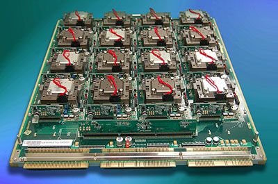
The in-house burn-in test solutions offered at KYEC are used to develop testing models that feature single carrier boards, regional carrier board or all carrier platforms. The current technological capabilities of KYEC can provide a variety of output powers to perform special group burn-in tests. The cutting-edge burn-in oven is applicable to logic products, CPU and chipsets. KYEC burn-in oven can satisfy diverse client needs. The burn-in test capacity of KYEC is the best worldwide in the industry.
KYEC uses Monitor Burn-In Oven for its burn-in system. IC signals can be monitored during burn-in tests. This machine has been used at KYEC for many years. The advantages include excellent quality, easy operation, and cost effectiveness. Furthermore, platform flexibility is superior. This system has contributed considerable production efficiency for our clients and is also one of our clients’ most preferred equipment.
Challenge
What Is The Challenge of High Power Burn In?
1. High currents can cause thermal control problems that causing voltage drops to affect the quality of the burn-in.
2. High current limits circuit board density, resulting in low yield and high cost.
Architecture of Socket Solution
1. Stanford O/T socket
2. Stanford O/T socket
3. Individual thermal control module
4. Individual power module
5. Individual DC converter